- Industries

Home Backup & Garden BMS
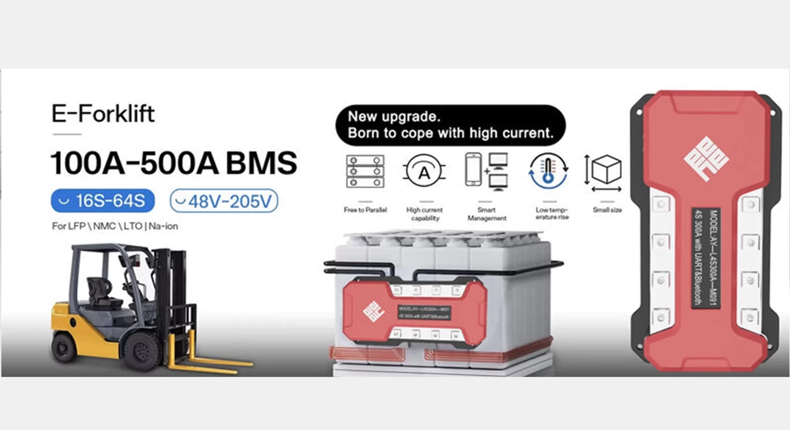
View More >Electric Forklift BMS
View More >Golf Cart BMS
View More >Electric Two-wheeler BMS
View More >Aviation & UAV BMS
View More >BMS For Power Tools
View More >Medical Equipment BMS
View More >


Home About Us EVENTS & NEWS The Role of PCB Design in High-Performance Power Systems and BMS
The efficiency, dependability, and safety of complex systems in modern electronics are largely determined by the PCB design process. Printed circuit boards (PCBs) are essential to any device that needs electrical connections, from satellites to cellphones. Because high-performance power systems and Battery Management Systems (BMS) require accuracy, stability, and fault tolerance, PCB design becomes even more important in these applications.
This article examines the types and structures of PCBs, their evolution, what PCB design is, and how advanced design techniques like HDI and UHDI have changed the field. We will also discuss the step-by-step design process, future trends that indicate smarter, more compact, and environmentally friendly solutions, and the role that PCB design plays in enabling improved BMS.

The engineering procedure used to create a printed circuit board’s physical layout is known as PCB design. Conductive paths, pads, and other features etched from copper sheets laminated onto a non-conductive substrate are used in PCBs, which are flat boards. Numerous electronic parts, including transistors, capacitors, diodes, integrated circuits, and connectors, are electrically connected by these channels.
Fundamentally, a PCB design makes sure that power and signals go freely between parts without interference, overheating, or mechanical failure. For example, accurate voltage sensing, current monitoring, and cell balancing in BMS systems depend on exact PCB design.
primitive single-layer boards were utilized for early consumer electronics and primitive radios in the early 20th century, marking the beginning of PCB technology. Engineers were forced to create multilayer boards, flexible circuitry, and high-density interconnects as a result of growing demands for dependability and downsizing.
In addition to supporting consumer electronics, PCB design is now a key component of the automotive, aerospace, renewable energy, and industrial automation sectors. As electric cars and renewable energy sources become more popular, BMS-powered systems depend on cutting-edge PCBs for both performance and safety.
Different PCB structures, each intended for a particular need, are used in modern applications. Typical varieties include:
Single-Sided PCB – One conductive copper layer; used in simple electronics.
Double-Sided PCB – Conductive layers on both sides, allowing more complex routing.
Multilayer PCB – Multiple stacked layers, widely used in power electronics and communication devices.
Rigid-Flex PCB – Combines rigid and flexible sections, suitable for compact and dynamic designs.
Flexible PCB – Entirely flexible, useful in wearable devices and sensors.
Printed Flexible PCB – Printed on polymer substrates for ultrathin applications.
Metal Core PCB (MCPCB) – Uses aluminum or copper as the base, ideal for high-power LEDs and thermal management.
Ceramic PCB – Excellent for high-frequency and high-temperature systems.
HDI PCB – High-density interconnect boards, enabling miniaturization with microvias.
UHDI PCB – Ultra-high-density interconnect PCBs, the frontier of compact and high-performance electronics.
Multilayer, HDI, and rigid-flex PCBs are frequently chosen for BMS applications because of their capacity to integrate power regulation, communication, and sensing in a small package.
A typical PCB consists of:
Substrate (FR4, ceramic, or metal core) – Provides mechanical support.
Copper Layers – Conduct electricity and signals.
Solder Mask – Protects copper traces and prevents short circuits.
Silkscreen – Prints labels for components.
The PCB design in high-performance power systems needs to manage:
High currents without excessive heating.
Low-noise signal transmission for sensors.
Integration with microcontrollers and communication interfaces.
Applications include improved medical gadgets, industrial robotics, electric cars, and renewable energy storage.
Blind, buried, and microvias are used in HDI PCB design to boost circuit density. Compact BMS modules in EV batteries require more components in smaller spaces, which is made possible by this. Additionally, HDI design lowers parasitics, increases signal integrity, and facilitates quicker component communication.
The state of the art in PCB design is represented by UHDI. It achieves line widths and spacings of less than 25 microns by utilizing advanced production technologies such as semi-additive processes (SAP). UHDI will enable previously unheard-of integration of wireless communication, protection, and sensing in a small footprint for future BMS designs.
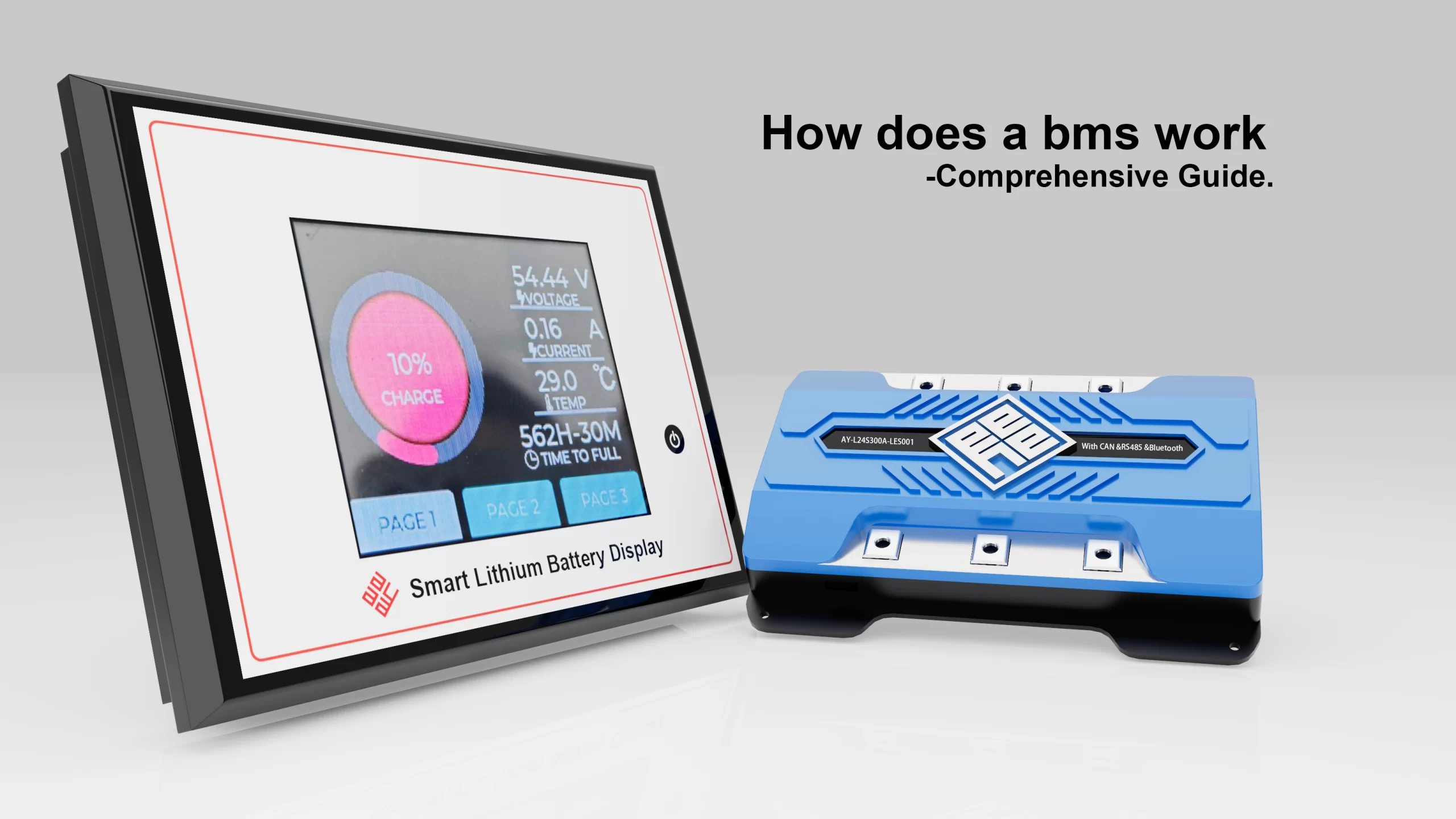
Any lithium-ion or sophisticated battery pack’s brain is called a Battery Management System (BMS). It balances cells, makes sure charging and discharging are safe, keeps an eye on variables like voltage, current, and temperature, and connects to other devices.
PCB design has a significant impact on a BMS’s performance:
Signal Accuracy – Ensures precise sensing of voltage and current.
Thermal Management – Avoids overheating through optimized copper thickness and thermal vias.
Isolation and Safety – Maintains separation between high-voltage and low-voltage sections.
Integration – Allows microcontrollers, communication chips (CAN, SMBus, Bluetooth), and protection MOSFETs to coexist seamlessly.
A BMS may not be able to protect batteries without an optimum PCB design, which could result in a shorter lifespan or safety risks.

These methods are used to design a dependable PCB for power systems or BMS:
Front-End Engineering – Define requirements, power ratings, and communication needs.
Schematic Capture – Map the logical circuit connections.
Material Selection and Stack-Up Design – Choose dielectric materials, copper thickness, and define the PCB layer stack.
Component Placement – Optimize placement for thermal flow and noise reduction.
Routing – Define signal paths, power traces, and high-current connections.
Design Review and Verification – Simulate thermal and signal performance.
Manufacturing Preparation – Generate Gerber files and fabrication instructions.
This PCB design process is streamlined by tools such as Altium Designer, which include simulation and rule-checking capabilities.
When it comes to high-performance power systems like EV drivetrains or grid-scale energy storage, PCB design guarantees:
High Current Handling – Wide traces, thick copper, and optimized via distribution.
Electromagnetic Compatibility (EMC) – Prevents noise from disrupting control electronics.
Reliability Under Stress – Resistant to vibration, thermal cycling, and high humidity.
These design decisions ensure power supply efficiency and safety when paired with BMS.
Environmental considerations must be incorporated into contemporary PCB design:
Eco-Friendly Materials – Lead-free solder and halogen-free laminates.
Energy Efficiency – Optimized routing to reduce power losses.
Lifecycle Costs – Though advanced PCBs are more expensive upfront, they reduce maintenance and extend system life.
Durable PCBs are especially advantageous for BMS-enabled battery systems since their longer lifespans lower waste and operating expenses.
In the future, PCB design will be influenced by:
Flexible and Wearable PCBs – For next-gen medical and consumer electronics.
3D Integrated Circuits – Stacking components vertically for higher density.
Neural-Inspired Architectures – PCBs tailored for AI and edge computing.
Smart PCBs with Embedded Sensors – Monitoring their own health for predictive maintenance.
These developments hold promise for BMS in the areas of wireless data transfer, intelligent diagnostics, and smooth cloud platform integration.
The PCB design process establishes the efficiency, safety, and functionality of contemporary systems; it is not just about joining parts. Optimized PCB architectures in high-performance power systems and BMS guarantee that batteries last longer, provide steady power, and stay safe under challenging circumstances.
AYAA TECH offers cutting-edge BMS products based on top-notch PCB knowledge for companies looking for innovative solutions. With advancements in CAN/SMBUS/Bluetooth communication, high-current handling, and worldwide application experience, AYAA TECH guarantees that your power systems and BMS solutions fulfill the most stringent performance and dependability requirements.
Q:What is the PCB design?
A:The process of developing the mechanical and electrical schematic for a printed circuit board (PCB), a hard framework that houses and joins electronic components to form a working circuit, is known as PCB design. Creating a schematic (circuit diagram), converting it into a physical layout, specifying component location and electrical connections (routing), and then producing manufacturing files are all steps in this intricate process. The objective is to create a circuit board that satisfies particular performance standards for a device while being practical, dependable, and reasonably priced.
Q:What are the three types of PCBs?
A:Single-sided, double-sided, and multi-layer PCBs are the three main varieties; each has unique properties, benefits, and drawbacks.
Q:What is the most common type of PCB?
A:The most popular kind of printed circuit board is a single-sided PCB. Above the substrate, there is a single layer of conductive copper. The complete engraved circuit is visible on one side of the board, while the electrical components are soldered or positioned on the other.
Q:What is the most used PCB design tool?
A:Altium Designer,Altium 365,PADS Professional,Allegro X PCB Designer,Autodesk Fusion.
Q:Do PCBs use AC or DC?
A:Direct current.
Contact Us